
Overview |
AMReX |
People |
Publications |
Microelectronics
Overview
What is ARTEMIS?
|
ARTEMIS is part of the two DOE-funded Microelectronics-CoDesign programs at Berkeley Lab
(Click here for the full list of awards) .
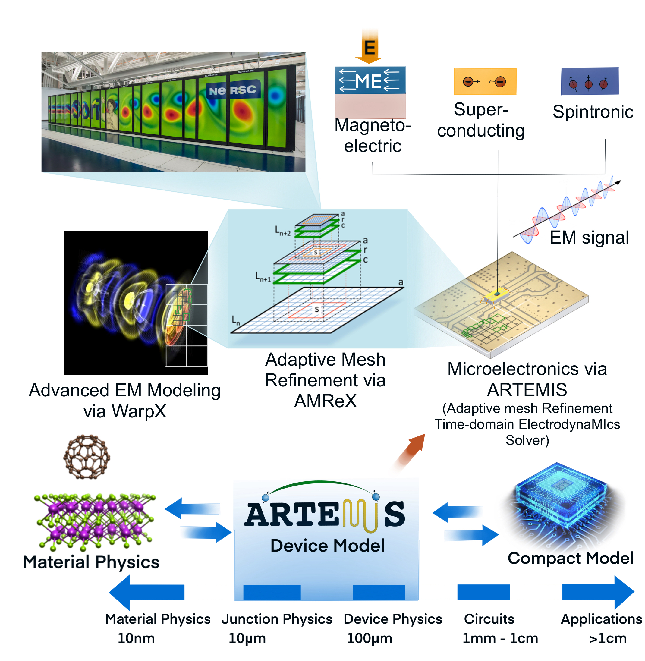
Overview of the device-level modeling capability, the ARTEMIS package.
ARTEMIS bridges the gap between material physics and circuit model of PARADISE, by solving governing PDEs of the physics in devices such as NCFET and MESO.
Since ARTEMIS is based off two ECP products, AMReX and WarpX, it fully functions on GPU supercomputers such as NERSC perlmutter system, providing rapid device-level modeling to the co-design workflow.
For more information about ARTEMIS or any of the applications below, contact the ARTEMIS Team or visit the ARTEMIS github page. |
ARTEMIS for Magnon-Photon Dynamics
ARTEMIS for Transmission Line Analysis
Modeling and characterization of electromagnetic wave interactions with microelectronic devices to derive network parameters has been a widely used practice in the electronic industry. However, as these devices become increasingly miniaturized with finer-scale geometric features, computational tools must make use of manycore/GPU architectures to efficiently resolve length and time scales of interest.
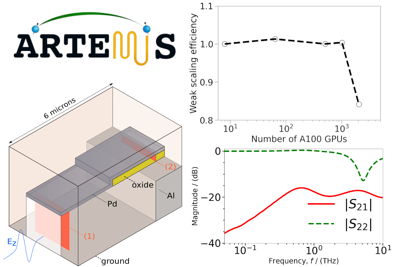
Left: A microscale transmission line with a Z-directional electric field excitation for computing S-matrix between ports (1) and (2). Bottom Right: Components of S-matrix as a function of frequency. Top Right: Weak-scaling efficiency of ARTEMIS on NVIDIA A100 GPUs using NERSC's Perlmutter supercomputer. |
This has been the focus of our open-source solver, ARTEMIS, which is performant on modern
GPU-based supercomputing architectures while being amenable to additional physics coupling. This work demonstrates its use
for characterizing network parameters of transmission lines using established techniques. A rigorous verification and
validation of the workflow is carried out, followed by its application for analyzing a transmission line on a CMOS chip
designed for a photon-detector application. Simulations are performed for millions of timesteps on state-of-the-art
GPU resources to resolve nanoscale features at gigahertz frequencies. The network parameters are used to obtain
phase delay and characteristic impedance that serve as inputs to SPICE models. The code is demonstrated to exhibit
ideal weak scaling efficiency up to 1024 GPUs and 84% efficiency for 2048 GPUs, which underscores its use for network
analysis of larger, more complex circuit devices in the future.
The details can be found in the following publication.
|
ARTEMIS for Superconducting Resonators
In collaboration with
Richard Lombardini of Saint Mary's University,
we have implemented a new London equation
module for superconductivity in the GPU-enabled ARTEMIS framework, and coupled it to a finite-difference
time-domain solver for Maxwell's equations. We applied this two-fluid approach to model a superconducting
coplanar waveguide (CPW) resonator and validated our implementation by verifying that the theoretical skin
depth and reflection coefficients can be obtained for several superconductive materials,
with different London penetration depths, over a range of frequencies. Our convergence studies show that
the algorithm is second-order accurate in both space and time. In our CPW simulations, we leverage the GPU
scalability of our code to compare the two-fluid model to more traditional approaches that approximate
superconducting behavior and demonstrate that superconducting physics can show comparable performance
to the assumption of quasi-infinite conductivity as measured by the Q-factor. The details can be found
in this recent publication.
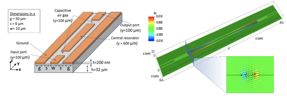 On the left is an illustration of a CPW resonator structure found in quantum readout applications with superconducting films sitting atop a silicon substrate.
The right depicts the spatial variation of electric field along an x-z slice passing through the transmission lines. The dark shaded regions indicate metal
(either conducting or superconducting). The red and blue shading indicates the magnitude of the Ex field (blue/red = +/-0.001 V/m) near the end of the simulation,
illustrating the fundamental mode. The inset is an x-z slice with normal in the y-direction extract at the front of the resonator line,
y = -300 microns, with vectors illustrating the electric field.
FerroX
FerroX is a massively parallel 3D phase-field simulation framework for modeling and design of
ferroelectric-based microelectronic devices. Due to their switchable polarization in response
to applied electric fields, ferroelectric materials have enabled a wide portfolio of innovative
microelectronics devices, such as ferroelectric capacitors, nonvolatile memories, and
ferroelectric field effect transistors (FeFET). FeFETs, in particular, are designed to
overcome the fundamental energy consumption limit (the "Boltzmann's Tyranny") associated
with individual semiconductor components, allowing for the design of ultra low-power logic
technologies. The goal of FerroX is to provide an in-depth insight into the underlying
physics and to facilitate researchers with a reliable design tool for novel microelectronic
devices. One of the key challenges in the modeling of devices such as FeFETs is the intrinsic
multiphysics nature of the multimaterial stacks. Typical ferroelectric devices involve at
least three coupled physical mechanisms: ferroelectric polarization switching, semiconductor
electron transport, and classical electrostatics, each of which includes rich underlying
physics. FerroX self-consistently couples the time-dependent Ginzburg Landau (TDGL) equation
for ferroelectric polarization, Poisson's equation for electric potential, and charge equation
for carrier densities in semiconductor regions. We discretize the coupled system of partial
differential equations using a finite difference approach, with an overall scheme that is
second-order accurate in both space and time. The algorithm is implemented using the AMReX
software framework, which provides effective scalability on manycore and GPU-based supercomputing
architectures. We have demonstrated the performance of the algorithm with excellent scaling
results on NERSC multicore and GPU systems, with a significant (15x) speedup on the GPU using
a node-by-node comparison. Additional details can be found
in this recent publication. Our ongoing efforts include implementation of the capability to
quantify the effect of tetragonal/orthorhombic phase mixtures in the negative capacitance
stabilization and effective oxide thickness lowering. In addition, we are adding features to
model carrier transport in semiconductor region to enable first full 3D simulation of FeFETs.
 MFISM stack with 5 nm thick HZO on top, followed by 1 nm thick SiO2, and a 10 nm thick Si as the ferroelectric, dielectric, and semiconductor layers, respectively. Vertical direction represents the thickness of the device (z). For an applied voltage, V app = 0 V (a) Polarization distribution showing multi-domain formation in HZO (b) Potential distribution induced in the semiconductor (c) Electric field vector plot in semiconductor.
ELEQTRONeX
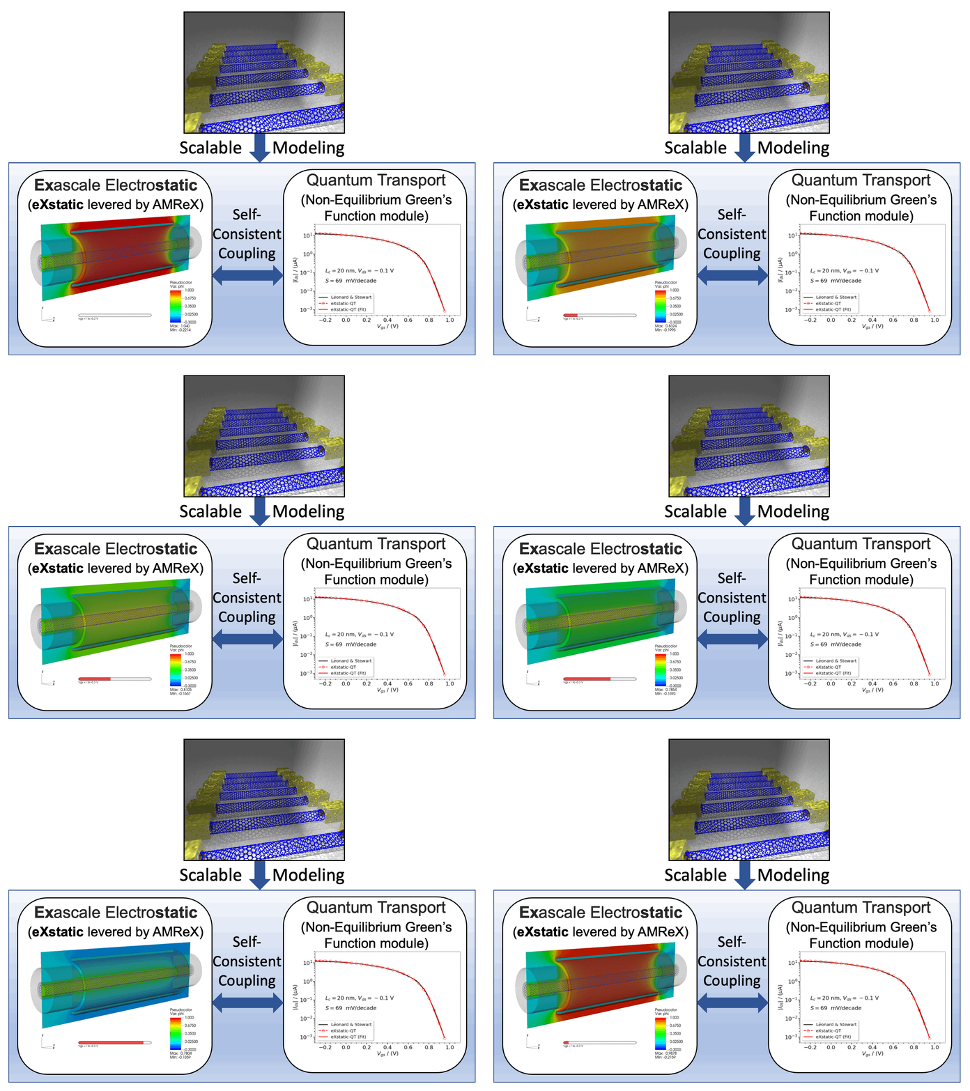
ELEQTRONeX is an exascale electrostatic-quantum transport framework currently supporting the modeling of carbon nanotube field-effect transistors (CNTFETs). It is developed as part of a DOE-funded project called 'Codesign and Integration of Nanosensors on CMOS.' One of the applications of CNTFETs is their use as sensors in advanced photodetectors, where carbon nanotubes are particularly attractive due to their high surface-to-volume ratio, making them highly sensitive to their environment. Such sensing applications require modeling arrays of nanotubes on the order of hundreds of nanometers in length, which may be functionalized with photosensing materials such as quantum dots. The goal of ELEQTRONeX is to model such systems, making efficient use of CPU/GPU heterogeneous architectures. The framework comprises three major components: the electrostatic module, the quantum transport module, and the part that self-consistently couples the two modules. The electrostatic module computes the electrostatic potential induced by charges on the surface of carbon nanotubes, as well as by source, drain, and gate terminals, which can be modeled as embedded boundaries with intricate shapes. The quantum transport module uses the nonequilibrium Green's function method to model induced charge. Currently, it supports coherent (ballistic) transport, contacts modeled as semi-infinite leads, and Hamiltonian representation using the tight-binding approximation. The self-consistency between the two modules is achieved using Broyden's modified second algorithm, which is parallelized on both CPUs and GPUs. Preliminary studies have demonstrated that the electrostatic and quantum transport modules can compute the potential on billions of grid cells and compute the Green's function for a material with millions of site locations within a couple of seconds, respectively.
MagneX
phononeX: Phonon Transport on Quantum Chips
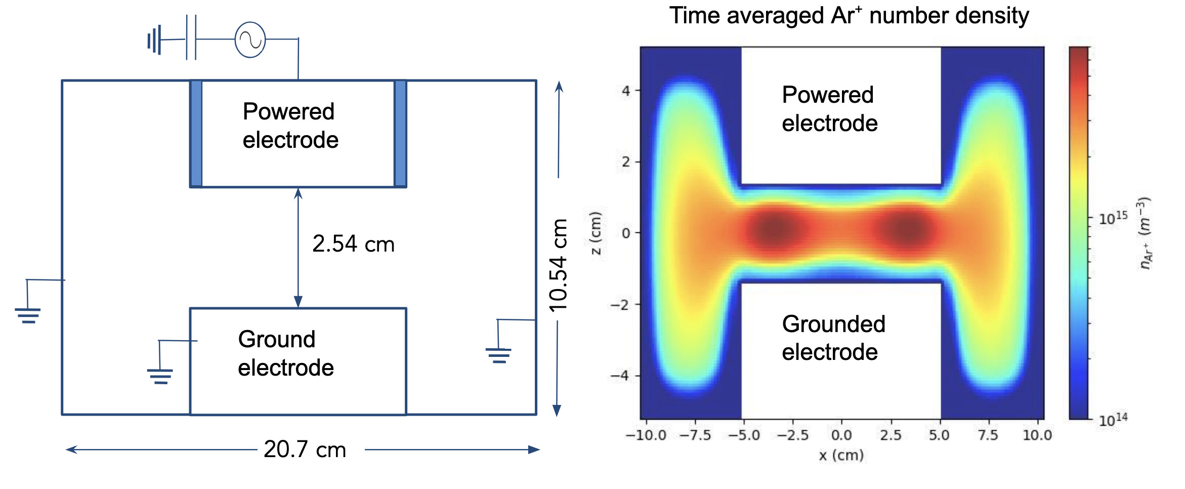
Plasma-Assisted Semiconductor Chip Fabrication
Machine Learning
Publications
 A. Nonaka, Y. Tang, J. C. LePelch, P. Kumar, W. Zhang, J. A. Munoz, C. Fernandez-Soria, C. Diaz, D. J. Gardner, and Z. Yao,
MagneX: A High-Performance, GPU-Enabled, Data-Driven Micromagnetics Solver for Spintronics,
submitted for publication.
[arXiv]
 Z. Yao, R. Cong, S. Husain, Y. Tang, T. Lee, A. Nonaka, J. Shalf, S. Salahuddin, L. Martin, K. Yang, and R. Ramesh,
Harnessing the Power of HPC and AI for Beyond-CMOS Microelectronics Device,
Proceedings of the 2025 IEEE International Electron Devices Meeting (IEDM), 2025.
[link]
 J. Song, Y. Tang, P. Ren, S. Takayoshi, S. Sawant, Y. Zhu, J.-M. Hu, A. Nonaka, M. W. Mahoney, B. Erichson, and Z. Yao,
HPC-Driven Modeling with ML-Based Surrogates for Magnon-Photon Dynamics in Hybrid Quantum System,
Proceedings of the 2025 International Applied Computational Electromagnetics Society Symposium (ACES), 2025
[link]
and
submitted for publication, 2025.
[arXiv]
 S. S. Sawant, T. Lara, F. Leonard, Z. Yao, and A. Nonaka,
Non-ideal subthreshold swing in aligned carbon nanotube transistors due to variable occupancy discrete charge traps,
submitted for publication, 2025.
[arXiv]
 Y. Tang, W. Xu, J. Cao, W. Gao, S. Farrell, B. Erichson, M. W. Mahoney, A. Nonaka, Z. Yao,
MatterChat: A Multi-Modal LLM for Material Science,
accepted for publication in Nature Machine Intelligence, 2026.
[arXiv]
 Y. Tang, R. Chen, M. Lou, J. Fan, C. Yu, A. Nonaka, Z. Yao., W. Gao,
Optical Neural Engine for Solving Scientific Partial Differential Equations,
Nature Communications, 16, 4603, 2025.
[doi]
 S. S. Sawant, F. Leonard, Z. Yao, A. Nonaka,
ELEQTRONeX: A GPU-Accelerated Exascale Framework for Non-Equilibrium Quantum Transport in Nanomaterials,
npj Comput. Materials, 11:110, 2025.
[link]
 P. Kumar, M. Hoffmann, A. Nonaka, S. Salahuddin, and Z. Yao
3D ferroelectric phase field simulations of polycrystalline multi-phase hafnia and zirconia based ultra-thin films,
Advanced Electronic Materials, 2400085, 2024.
[link]
 R. Jambunathan, Z. Yao, R. Lombardini, A. Rodriguez, and A. Nonaka,
Two-Fluid Physical Modeling of Superconducting Resonators in the ARTEMIS Framework,
Computer Physics Communications, 291, 2023.
[link]
 P. Kumar, A. Nonaka, R. Jambunathan, G. Pahwa, S. Salahuddin, and Z. Yao,
FerroX: A GPU-accelerated, 3D Phase-Field Simulation Framework for Modeling Ferroelectric Devices,
Computer Physics Communications, 108757, 2023.
[link]
 S. Sawant, Z. Yao, R. Jambunathan, and A. Nonaka,
Characterization of Transmission Lines in Microelectronics Circuits using the ARTEMIS Solver,
IEEE J. on Multiscale and Multiphysics Comp. Tech., 8, 2022.
[link]
 Z. Yao, R. Jambunathan, Y. Zeng, and A. Nonaka,
A Massively Parallel Time-Domain Coupled Electrodynamics-Micromagnetics Solver,
International Journal of High Performance Computing Applications, 10943420211057906, 2021.
[link]